Researchers have unveiled a new photonic in-memory computing method that promises to advance optical computing significantly.
This technology, using magneto-optical materials, achieves high-speed, low-energy, and durable memory solutions suitable for integration with existing computing technologies.
Photonic In-Memory Computing
For the first time, a global team of electrical engineers has developed a new method for photonic in-memory computing, bringing optical computing closer to becoming a reality.
The team includes researchers from the University of Pittsburgh Swanson School of Engineering, the University of California – Santa Barbara, the University of Cagliari, and the Tokyo Institute of Technology (now the Institute of Science Tokyo). Their results were published on October 23 in the journal Nature Photonics (“Integrated non-reciprocal magneto-optics with ultra-high endurance for photonic in-memory computing.”
This research was a collaborative effort led by Nathan Youngblood, assistant professor of electrical and computer engineering at Pitt, along with Paulo Pintus, formerly of UC Santa Barbara and now an assistant professor at the University of Cagliari, and Yuya Shoji, associate professor at the Institute of Science Tokyo.
Overcoming Optical Memory Limitations
Until now, researchers have been limited in developing photonic memory for AI processing – gaining one important attribute like speed while sacrificing another like energy usage. In the article, the international team demonstrates a unique solution that addresses current limitations of optical memory that have yet to combine non-volatility, multibit storage, high switching speed, low switching energy, and high endurance in a single platform.
“The materials we use in developing these cells have been available for decades. However, they have primarily been used for static optical applications, such as on-chip isolators rather than a platform for high-performance photonic memory,” Youngblood explained. “This discovery is a key enabling technology toward a faster, more efficient, and more scalable optical computing architecture that can be directly programmed with CMOS (complementary metal-oxide semiconductor) circuitry – which means it can be integrated into today’s computer technology.
“Additionally, our technology showed three orders of magnitude better endurance than other non-volatile approaches, with 2.4 billion switching cycles and nanosecond speeds.”
Introducing a Resonance-Based Architecture
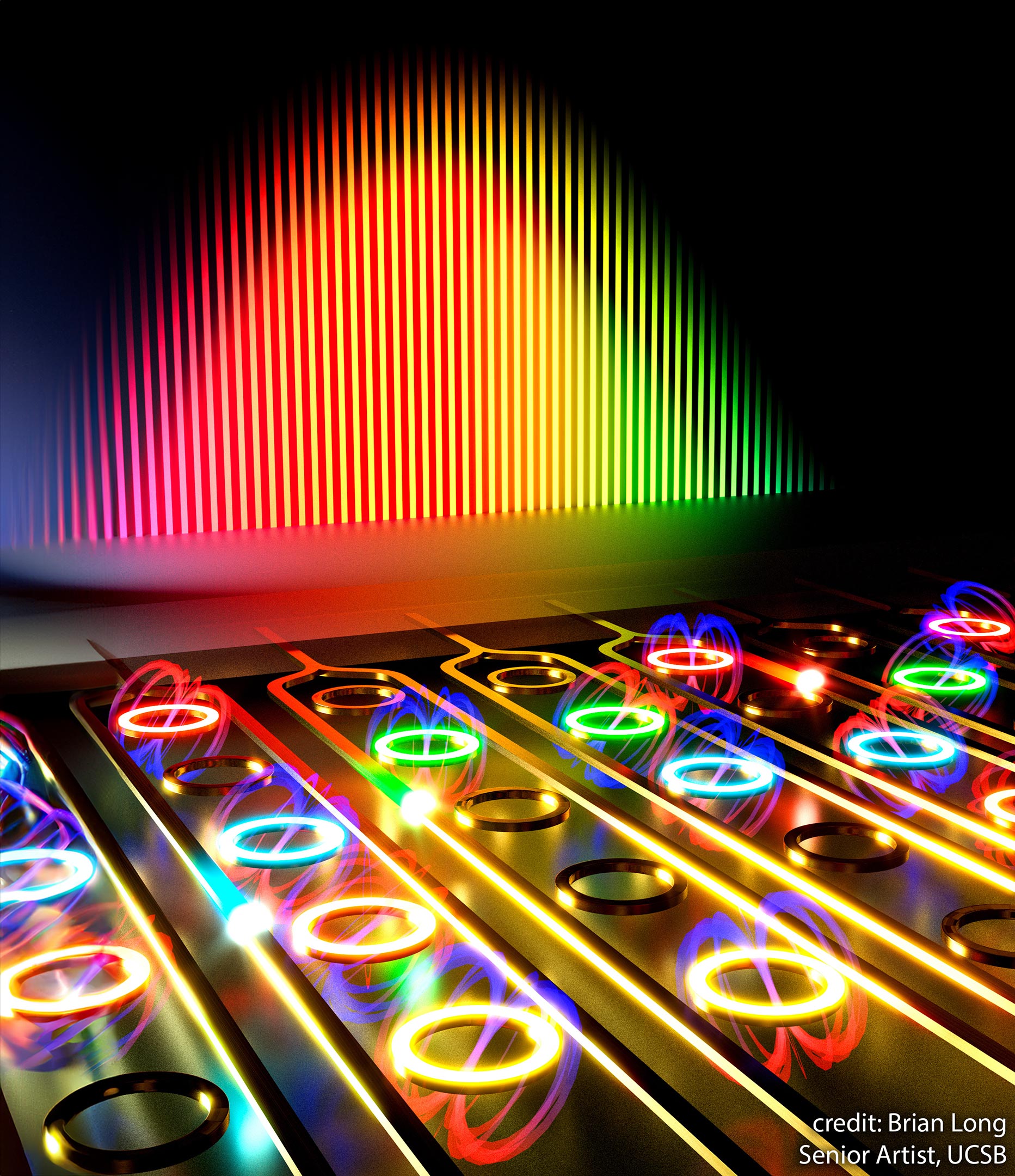
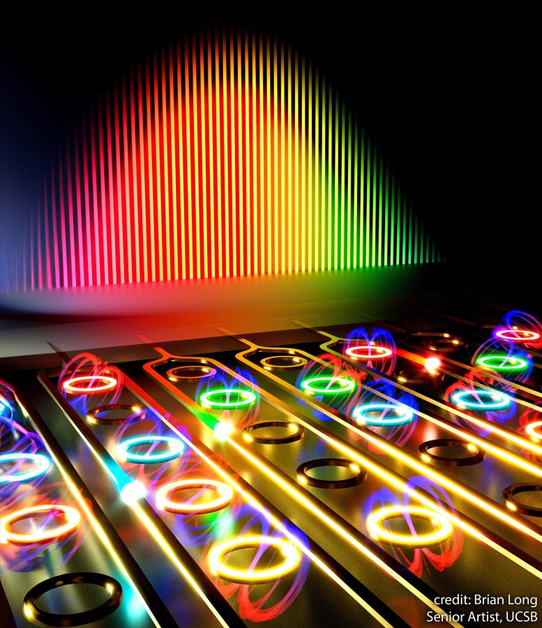
The authors propose a resonance-based photonic architecture that leverages the non-reciprocal phase shift in magneto-optical materials to implement photonic in-memory computing.
A typical approach to photonic processing is to multiply a rapidly changing optical input vector with a matrix of fixed optical weights. However, encoding these weights on-chip using traditional methods and materials has proven challenging. By using magneto-optic memory cells comprised of heterogeneously integrated cerium-substituted yttrium iron garnet (Ce:YIG) on silicon micro-ring resonators, the cells cause light to propagate bidirectionally, like sprinters running opposite directions on a track.
Computing by Controlling the Speed of Light
“It’s like the wind is blowing against one sprinter while helping the other run faster,” explained Pintus, who led the experimental work at UC Santa Barbara. “By applying a magnetic field to the memory cells, we can control the speed of light differently depending on whether the light is flowing clockwise or counterclockwise around the ring resonator. This provides an additional level of control not possible in more conventional non-magnetic materials.”
Future Prospects and Scaling
The team is now working to scale up from a single memory cell to a large-scale memory array which can support even more data for computing applications. They note in the article that the non-reciprocal magneto-optic memory cell offers an efficient non-volatile storage solution that could provide unlimited read/write endurance at sub-nanosecond programming speeds.
“We also believe that future advances of this technology could use different effects to improve the switching efficiency,” Shoji at Tokyo added, “and that new fabrication techniques with materials other than Ce:YIG and more precise deposition can further advance the potential of non-reciprocal optical computing.”
Reference: “Integrated non-reciprocal magneto-optics with ultra-high endurance for photonic in-memory computing” by Paolo Pintus, Mario Dumont, Vivswan Shah, Toshiya Murai, Yuya Shoji, Duanni Huang, Galan Moody, John E. Bowers and Nathan Youngblood, 23 October 2024, Nature Photonics.
DOI: 10.1038/s41566-024-01549-1
Other researchers on this project include:
- John E. Bowers, distinguished faculty at University of California at Santa Barbara
- Mario Dumont, graduate student researcher at University of California at Santa Barbara
- Duanni Huang, former researcher at University of California at Santa Barbara
- Galan Moody, faculty at University of California at Santa Barbara
- Toshiya Murai, researcher at National Institute of Advanced Industrial Science and Technology, Japan
- Vivswan Shah, graduate student researcher at University of Pittsburgh
N.Y. acknowledges support from the National Science Foundation under grant nos. ECCS-2210168/2210169 and CISE-2105972. N.Y. acknowledges support from the University of Pittsburgh Center for Research Computing (grant no. RRID:SCR_022735) via the resources provided. Specifically, this work used the H2P cluster, which is supported by NSF award no. OAC-2117681.
P.P., G.M., and J.E.B. acknowledge support from the Air Force Office of Scientific Research under award nos. FA9550-21-1-0042 and FA9550-20-1-0150. P.P. also acknowledges support from the Autonomous Region of Sardinia via the ‘Mobilità Giovani Ricercatori (MGR)’ program of the University of Cagliari; the Italian Ministry of University and Research via the PRIN PNRR 2022 project ‘Magneto-optic Integrated Computing (MAGIC)’ (grant no. CUP F53D23008340001); and the Fondazione di Sardegna via the ‘Investigation of Novel Magneto-Optic Materials and Devices for Silicon Photonic Integrated Circuits’ project (grant no. CUP F73C23001820007). Any opinions, findings, conclusions, or recommendations expressed in this material are those of the authors and do not necessarily reflect the views of the US Air Force.