

Researchers at Berkeley Lab have advanced the understanding of magnetic skyrmions by developing techniques to image their 3D structures.
These nanoscale objects show promise for revolutionizing microelectronics through enhanced data storage capabilities and reduced energy consumption.
A difficult-to-describe nanoscale structure called the magnetic skyrmion holds potential for creating advanced microelectronic devices, including those with vast data storage capacities and significantly lower power requirements.
However, to reliably integrate skyrmions into future computational devices—potentially even quantum computers—researchers need a more thorough understanding of their properties. Peter Fischer, a senior researcher at the Department of Energy’s Lawrence Berkeley National Laboratory (Berkeley Lab), led a project using 3D X-ray imaging to capture detailed views of skyrmions, specifically measuring the orientations of their magnetic spins throughout the entire object. “Our results provide a foundation for nanoscale metrology for spintronics devices,” Fischer said. This work was recently published in Science Advances.
“Our results provide a foundation for nanoscale metrology for spintronics devices.”
Peter Fischer
Characteristics and Potential of Skyrmions
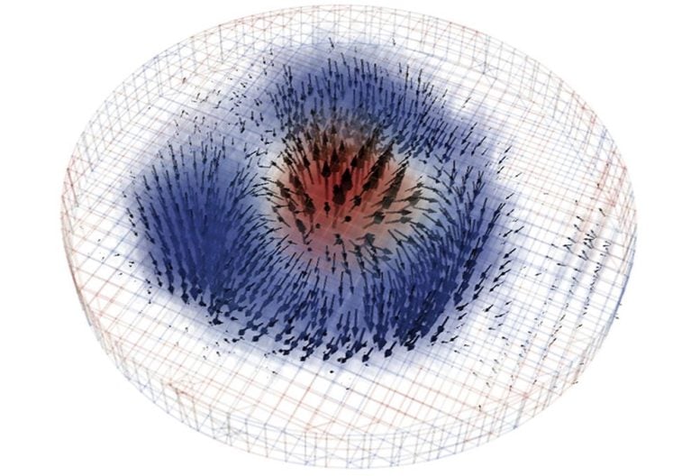
Magnetic skyrmions can be thought of as spinning circles of magnetism, explains David Raftrey, a student researcher in Fischer’s team who was the lead author of this study. At the center, the magnetic spin is pointing upward, while moving out from the center, the magnetism twists and pulls in a downward direction. What’s more, skyrmions are stable, small, fast, and not easily unfolded, a trait materials scientists dub “topological.”
These spin directions are part of the appeal for skyrmions because they might be used to carry and store information in much the same way that electrons carry and store information in current devices. “However, relying on the charge of the electron, as it is done today, comes with inevitable energy losses. Using spins, the losses will be significantly lower,” Fischer said.
Exploring 3D Structures of Skyrmions
Theoretical knowledge of skyrmions has been based on descriptions of them as 2D objects. However, in the real world of electronics and silicon wafers — no matter how thin — skyrmions have to be dealt with as 3D objects. To put skyrmions to work, or perhaps to one day synthesize custom skyrmions, researchers must be able to examine and understand their spin characteristics throughout the whole 3D object.
If you are looking at a skyrmion magnetic whirlpool from the top and start slicing off layers, you might think that each successive layer would be the same. “But that’s not the case,” Raftrey said. “And we said, okay, how can we get our arms around this? How do we actually demonstrate this?”
Breakthrough in Skyrmion Research
Raftrey took a thin magnetic layer, which was synthesized by colleagues from Western Digital, and patterned a nanodisk using the Molecular Foundry’s nanofabrication facility. To obtain 3D tomographic images he traveled to Switzerland to use a novel imaging technique called magnetic X-ray laminography at a microscopy beamline at the Swiss Light Source.
With X-ray laminography, “You can basically reconfigure and reconstruct [the skyrmion] from these many, many images and data,” Raftrey said. It was a process that took months, finally yielding a better understanding of skyrmion spin structures.
A full understanding of skyrmions’ 3D spin texture “opens opportunities to explore and tailor 3D topological spintronic devices with enhanced functionalities that cannot be achieved in two dimensions,” Fischer said.
Reference: “Quantifying the topology of magnetic skyrmions in three dimensions” by David Raftrey, Simone Finizio, Rajesh V. Chopdekar, Scott Dhuey, Temuujin Bayaraa, Paul Ashby, Jörg Raabe, Tiffany Santos, Sinéad Griffin and Peter Fischer, 2 October 2024, Science Advances.
DOI: 10.1126/sciadv.adp8615
The Molecular Foundry is a DOE Office of Science user facility at Berkeley Lab.
The work was supported by the DOE Office of Science.