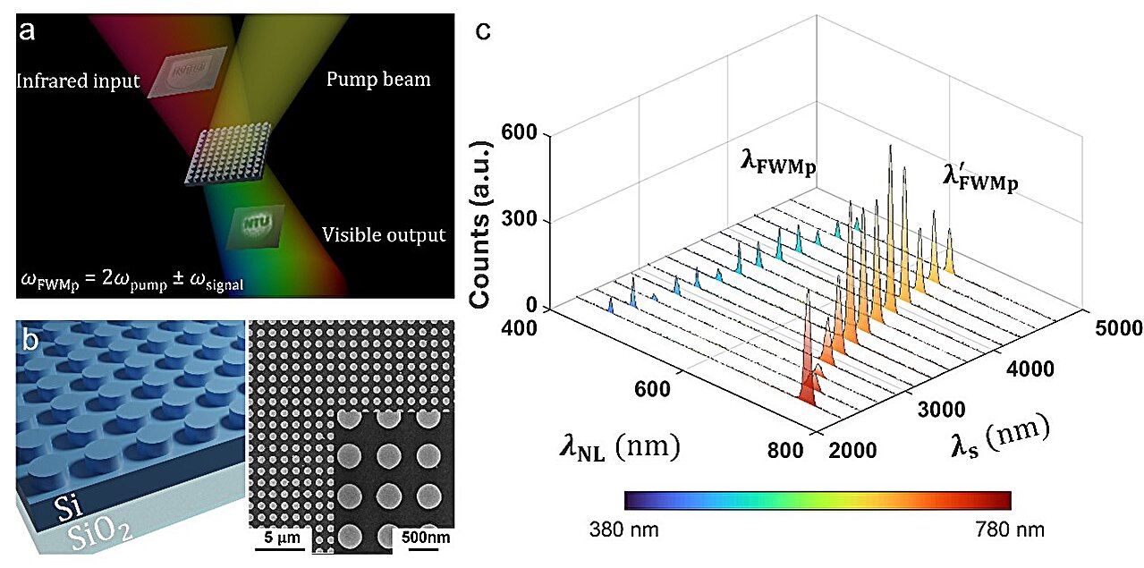
 processes. b, Left: The schematic diagram of Si bi-layer metasurface. Right: Scanning electron microscopy images of the metasurface from the top. c, The measured FWM emission spectra from Si metasurface while tuning the signal wavelength when fixing the pump wavelength at 1130 nm. The tuning ranges of the signal wavelength are from 2300 to 4700 nm. Credit: by Ze Zheng, Daria Smirnova, Gabriel Sanderson, Cuifeng Ying, Demosthenes C. Koutsogeorgis, Lujun Huang, Zixi Liu, Rupert Oulton, Arman Yousefi, Andrey E. Miroshnichenko, Dragomir N. Neshev, Mary O'Neill, Mohsen Rahmani, and Lei Xu")
Infrared imaging technology is crucial for advancing our understanding of the world, from exploring biological specimens to inspecting complex materials and detecting hidden patterns in physical systems.
Infrared light can penetrate fog and smoke, making it invaluable for search and rescue, firefighting, and sensitive operations. Additionally, infrared imaging can enable visualizing the heat emitted by objects, making it a powerful tool for night vision and security applications.
While infrared cameras are valuable tools for enhanced vision, food and plant quality control, security, etc, today’s cameras often face significant drawbacks. For instance, they are bulky and power-hungry, requiring cooling systems that limit their functionalities.
More importantly, current semiconductor-based technology used in the cameras only captures a narrow band of the infrared spectrum based on the absorption band of the semiconductor detector. This means that every application would need a separate camera.
“Due to the complications of today’s bulky, power-hungry and expensive infrared imaging technology, we are unlikely to have an infrared camera at home. However, nonlinear frequency conversion, a process that manipulates and translates electromagnetic signals across various frequency regimes, holds a massive potential to revolutionize infrared detection technology,” said Prof Mohsen Ramhami, the leader of Advanced Optics and Photonics Lab, and a UK Research and Innovation Future Leaders Fellow.
“We have demonstrated that arrays of engineered silicon nanoparticles called metasurfaces can convert infrared light into visible light through a frequency mixing process. Such metasurfaces that are integrable to regular cameras offer a promising solution for advanced infrared imaging.”
The silicon industry, known for producing compact electronic chips and circuits with excellent uniformity and being compatible with complementary metal oxide-sensitive (CMOS) packaging techniques, is an established industry today. Silicon photonics is a sub-industry mainly focused on fiber optics, waveguides, and telecommunications devices.
However, silicon nanoparticles and metasurfaces’ applications are relatively newer focus areas, particularly in the nonlinear regime, facilitating seamless light coupling between free-space environments and integrated circuitry.
In a paper published in Light: Science & Applications, an international team led by Nottingham Trent University has demonstrated one more advanced application of silicon metasurfaces: an affordable, compact, and versatile solution to realizing broadband infrared imaging.
The leading author, Ze Zheng, Ph.D. candidate at Nottingham Trent University, says, “Our demonstration benefits from an innovative and meticulous arrangement of silicon metasurface featuring a bi-layer device with silicon nanoparticles on top and silicon thin film underneath.
“By employing the light-matter interaction with both layers and interference of the resonances generated in both layers, we managed to induce multiple hybrid resonances, which significantly enhanced Four-Wave Mixing (FWM) across a broad wavelength range. This enhancement allows the detection of weak infrared signals, thanks to the quadratic power dependence of the nonlinear emission on the pump beam.”
As a proof of concept, the team has demonstrated that such an FWM-based imaging platform can enable the detection of sample thicknesses by measuring the time delays of the mixed infrared lights after passing through the sample.
Furthermore, this technique is polarization-selective, offering additional functions, such as detecting materials sensitive to polarization and enhancing the resolution and sensitivity for surface detection.
Associate Professor Lei Xu, the project’s co-leader, says, “Our infrared imaging across 1,000–4,700 nm with one device demonstrates new possibilities for developing broadband and compact devices for infrared imaging.
“This opens up a new research and development direction to address the current limitations of infrared cameras, such as high cost, complexity, and narrow bandwidth. This is the first step to make the next generation of infrared cameras more accessible and efficient.”
More information:
Ze Zheng et al, Broadband infrared imaging governed by guided-mode resonance in dielectric metasurfaces, Light: Science & Applications (2024). DOI: 10.1038/s41377-024-01535-w
Provided by
Chinese Academy of Sciences
Citation:
Silicon metasurfaces unlock broad-spectrum infrared imaging (2024, October 16)
retrieved 17 October 2024
from https://phys.org/news/2024-10-silicon-metasurfaces-broad-spectrum-infrared.html
This document is subject to copyright. Apart from any fair dealing for the purpose of private study or research, no
part may be reproduced without the written permission. The content is provided for information purposes only.