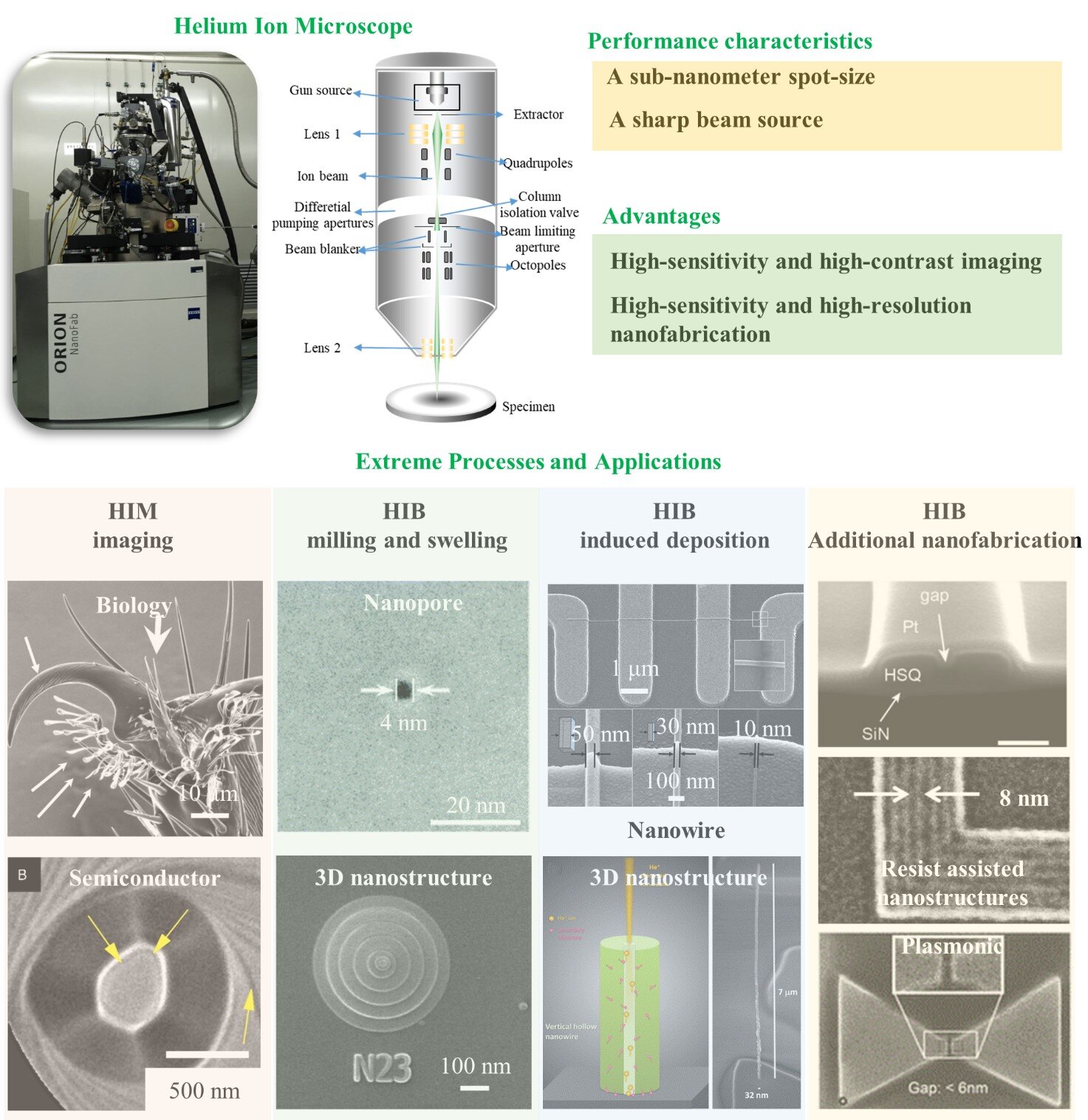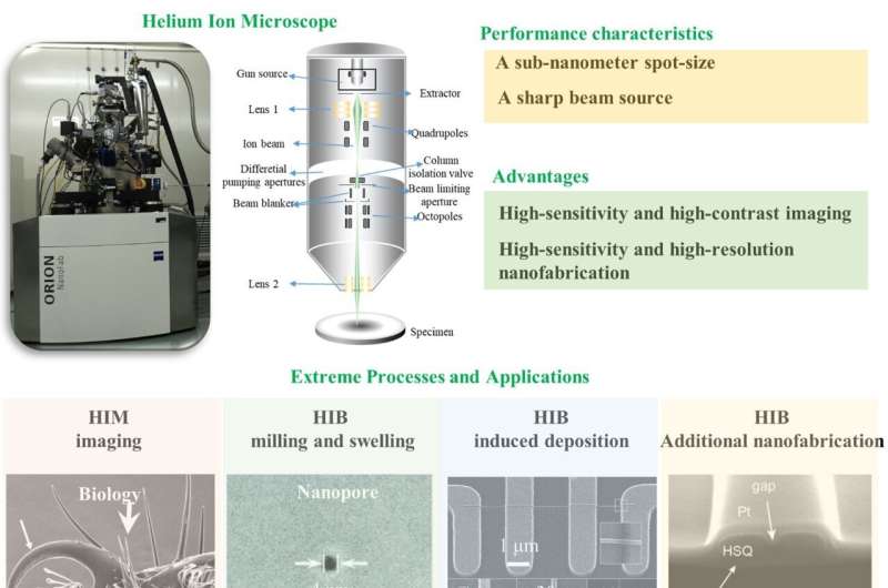

Helium ion beam (HIB) technology plays an important role in the extreme fields of nanofabrication. Due to high resolution and sensitivity, HIB nanofabrication technology is widely used to pattern nanostructures into components, devices, or systems in integrated circuits, materials sciences, nano-optics, and bio-sciences applications. HIB-based nanofabrication includes direct-write milling, ion beam-induced deposition, and direct-write lithography without the need to resist assistance. Their nanoscale applications have also been evaluated in the areas of integrated circuits, materials sciences, nano-optics, and biological sciences.
In a new paper published in the International Journal of Extreme Manufacturing, a team of researchers, led by Dr. Deqiang Wang from Chongqing Key Laboratory of Multi-scale Manufacturing Technology, Chongqing Institute of Green and Intelligent Technology, Chinese Academy of Sciences, PR China, have summarized comprehensively the extreme processes and applications of HIB nanofabrication.
The main aim of this review is to address the latest developments in HIB technology with their extreme processing capabilities and widespread applications in nanofabrication. Based on the introduction of the HIM system with GFIS, the performance characteristics and advantages of HIB technology have been discussed first. Thereafter, certain questions about the extreme processes and applications of HIB nanofabrication have been addressed: How many extreme processes and applications of HIB technology have been developed in nanofabrication for integrated circuits, materials sciences, nano-optics, and bio-sciences applications? What are the main challenges in the extreme nanofabrication with HIB technology for high resolution and sensitivity applications?
HIM has the advantages of high resolution and sensitivity for extreme nanostructures fabrications. HIB-based nanofabrication includes direct-write milling, ion beam-induced deposition, and direct-write lithography without the need to resist assistance. Their nanoscale applications have also been evaluated in the areas of integrated circuits, materials sciences, nano-optics, and biological sciences. This review mainly covers four thematic applications of HIB: 1) helium ion microscopy (HIM) imaging for biological samples and semiconductors; 2) HIB milling and swelling for 2D/3D nanopore fabrication; 3) HIB-induced deposition for nanopillars, nanowires, and 3D nanostructures; 4) additional HIB direct writing for resist, graphene, and plasmonic nanostructures.
HIB technology is used for high-contrast, high-resolution imaging of conductive, semiconductor, insulating materials, and biological samples. Although the ions collide with the target sample, it will be better than conventional SEM imaging. The focused HIB technology has distinct advantages in nanofabrication, including milling processes for local thickness control and nanostructures fabrication in free-standing membranes or bulk materials. However, the amorphization and helium implantation may cause sample damage during HIB milling on bulk substrates. Therefore, the optimization of ion dose, beam energy, and HIB dose rate is critical for local thickness manipulation and topography accuracy control in nanostructures fabrication. Ion beam-induced deposition is an important nanofabrication technology, which can modify the properties of materials according to the interaction between the ion beam and materials. The development of HIB-induced deposition is a reasonable, appropriate technique for these specific nanofabrication applications because of the light mass of helium ions and the different electrical properties between inert helium and electroactive gallium. Due to the sub-nanometer spot size, the focused HIB is employed as a new, high-resolution direct writing exposure beam for nanofabrication. According to its high resolution, high SE yield, and low proximity effect, HIB direct writing is equal to or better than electron beam lithography for nanoelectronic device fabrication. Moreover, due to the relatively low mass, helium ions are less damaged than other particles such as electrons, and gallium ions for exposed target substrates.
Professor Deqiang Wang (Director of Chongqing Key Laboratory of Multi-scale Manufacturing Technology, CIGIT), Professor Wen-Di Li, Professor Wei Wu, Dr. Shixuan He, and Dr. Rong Tian have identified a few critical challenges in the extreme processes and applications of HIB nanofabrication as follows:
“For extreme nanofabrication, nanometer-scale nanopores that are beneficial for single base recognition of DNA/RNA sequences can be fabricated by HIB milling on thinned silicon nitride membrane or suspended graphene. Amorphization during the milling process promotes the formation of specific 3D nanopores, which can be used for potential nano-optics and bioscience applications.”
“The chemical reaction of the precursor gas molecules adsorbed on the surface induced by HIB results in the direct deposition of programmed 3D structures at the nanoscale.”
“HIB direct writing without resist-assisted is used to pattern sub-10-nm nanochannels, nanoribbons, and nanostructures for nanoscale functional devices.”
“Both HIM imaging and HIB nanofabrication must take into account the inevitable damage which is caused by the collision between helium ions and probe substrate. HIB technology has a lower sputtering yield but can produce larger damage on the substrate in nanofabrication processing, such as bubbles, implantation, and amorphization. More in-depth theoretical research on the interaction mechanism between helium ions and materials has promoted the improvement of the processing capability of the extreme nanofabrication with HIB technology.”
“The stability and repeatability of the HIB milling process will be enhanced to meet the requirements of sub-nanometer resolution and high-throughput fabrication in special applications. When optimizing the nanofabrication process, the positive or negative impact of helium ions bombardment on the material properties should be considered, so that HIB technology can be used to directly fabricate nanostructures with fewer defects and excellent performance.”
“For direct-write HIB technique and HIB-induced deposition processes, the common challenge is to increase the complexity of nanostructures while maintaining the nanoscale feature size for the special applications. To increase the complexity of nanostructures and their applications in production, the direct writing process of HIB technology must be improved through careful optimization of parameters. Besides, the proximity effect should be also taken into consideration in the HIB direct writing and HIB-induced deposition processes.”
Researchers have demonstrated that HIB technology will play an important role in extreme nanofabrication because it has the advantages of high sensitivity, resolution, and precision for direct writing milling, patterning, assisted-milling, and deposition processes with fewer damages to the samples.
How to draw a line narrower than a cold virus
Shixuan He et al, Helium-ion-beam nanofabrication: extreme processes and applications, International Journal of Extreme Manufacturing (2020). DOI: 10.1088/2631-7990/abc673
Provided by
International Journal of Extreme Manufacturing
Citation:
Helium-ion-beam nanofabrication: Extreme processes and applications (2022, July 29)
retrieved 29 July 2022
from https://phys.org/news/2022-07-helium-ion-beam-nanofabrication-extreme-applications.html
This document is subject to copyright. Apart from any fair dealing for the purpose of private study or research, no
part may be reproduced without the written permission. The content is provided for information purposes only.