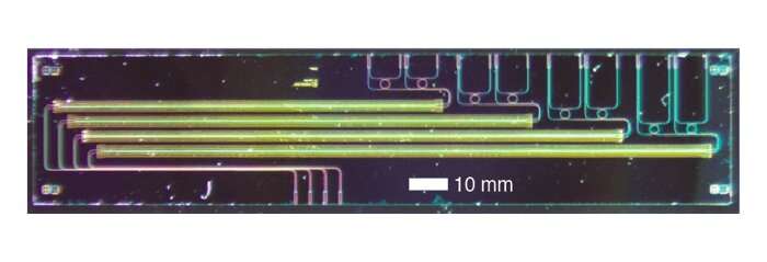

An optical isolator developed at the Harvard John A. Paulson School of Engineering and Applied Sciences (SEAS) could drastically improve optical systems for many practical applications.
All optical systems—used for telecommunications, microscopy, imaging, quantum photonics, and more—rely on a laser to generate photons and beams of light. To prevent those lasers from damage and instability, these systems also require isolators, components that prevent light from traveling in undesired directions. Isolators also help cut down on signal noise by preventing light from bouncing around unfettered. But conventional isolators have been relatively bulky in size and require more than one type of material to be joined together, creating a roadblock to achieving enhanced performance.
Now, a team of researchers led by electrical engineer Marko Lončar at SEAS has developed a method for building a highly-efficient integrated isolator that’s seamlessly incorporated into an optical chip made of lithium niobate. Their findings are reported in Nature Photonics.
“We constructed a device that lets light emitted by the laser propagate unaltered, while the reflected light that travels back towards the laser changes its color and gets re-routed away from the laser,” said Lončar, Tiantsai Lin Professor of Electrical Engineering at SEAS. “This is accomplished by sending electrical signals in the direction of the reflected optical signals, thus taking advantage of the excellent electro-optic properties of lithium niobate,” in which voltage can be applied to change the properties of optical signals, including speed and color.
“We wanted to create a safer environment for a laser to operate in, and by designing this one-way street for light, we can protect the device from the laser’s reflection,” said Mengjie Yu, co-first author on the paper and a former postdoctoral researcher in Lončar’s lab. “To our knowledge, when compared to all other demonstrations of integrated isolators, this device performs the best optical isolation in the world. In addition to isolation, it offers the most competitive performance across all metrics including loss, power efficiency, and tunability.”
“What’s exceptional about this device is that at its core it’s incredibly simple—it’s really just one single modulator,” says Rebecca Cheng, co-first author on the paper and a current Ph.D. student in Lončar’s lab. “All previous attempts at engineering something like this required multiple resonators and modulators. The reason we can do this with such remarkable performance is because of lithium niobate’s properties.”
Another reason for the high performance and efficiency has to do with the size of the device—the team built it at the Harvard Center for Nanoscale Systems, fabricating a chip measuring 600 nanometers thick with etchings (to guide the light using prescribed nanostructures) up to 320 nanometers deep.
“With a smaller device, you can control light more easily and also put that light in closer proximity to the electrical signals, thus achieving a stronger electrical field with the same voltage,” enabling more powerful control of light, Yu said.
The scaled-down dimensions and ultralow loss property of this platform also boost optical power. “Since the light doesn’t have to travel so far, there is less decay and loss of power,” Cheng said.
Finally, the teams show the device can successfully protect an on-chip laser from external reflection. “We are the first team to show the laser’s phase-stable operation under the protection of our optical isolator,” said Yu.
Altogether, the advance represents a significant leap forward for practical, high-performance optical chips. The team reports that it can be used with a range of laser wavelengths, only requiring a counter-propagating electrical signal to achieve the desired effects.
The team hopes the breakthrough—part of a larger effort to integrate lasers and photonics components on a chip at extremely small scales—will unlock new capabilities in a range of applications, spanning the telecommunications industry to time-frequency transfer, a way of precisely measuring time down to the atomic and sub-atomic scale that could have implications for quantum research and computing.
“Integrating all aspects of an optical system onto a single chip could replace many larger, more costly, and less efficient systems,” Yu said. “Combining all these things could revolutionize many fields of work.”
More information:
Mengjie Yu et al, Integrated electro-optic isolator on thin-film lithium niobate, Nature Photonics (2023). DOI: 10.1038/s41566-023-01227-8
Provided by
Harvard John A. Paulson School of Engineering and Applied Sciences
Citation:
Engineers develop first-of-its-kind integrated optical isolator (2023, June 29)
retrieved 29 June 2023
from https://phys.org/news/2023-06-first-of-its-kind-optical-isolator.html
This document is subject to copyright. Apart from any fair dealing for the purpose of private study or research, no
part may be reproduced without the written permission. The content is provided for information purposes only.

