
Sandia National Laboratories and Arizona State University are enhancing quantum technology by miniaturizing optical systems into chip-sized integrated microsystems.
This partnership aims to leverage advanced photonics for quantum computing and secure communications, highlighted by a new initiative funded by the Quantum Collaborative.
Collaborative Quantum Innovations
Sandia National Laboratories and Arizona State University, two leading research institutions, are working together to advance quantum technology by shrinking large optical systems into compact integrated microsystems.
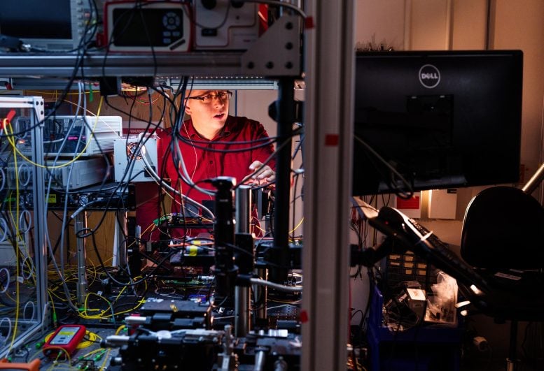
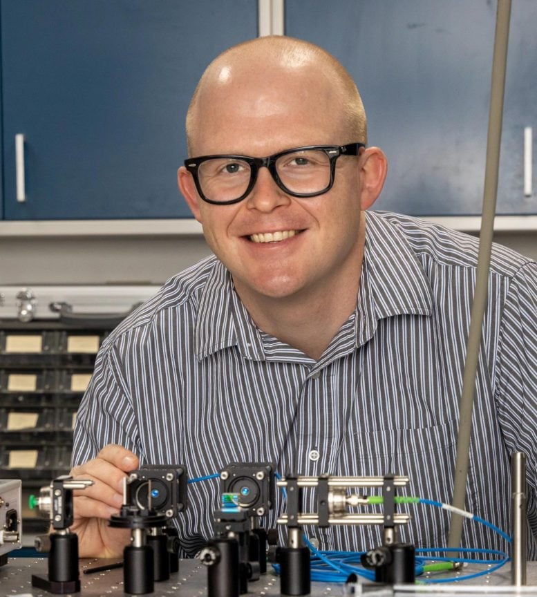
Nils Otterstrom, a physicist at Sandia who specializes in integrated photonics, is leading efforts to miniaturize these optical systems. This breakthrough promises enhanced performance and scalability, with applications ranging from advanced computing to secure communications.
“Integrated photonics takes optical systems that are macroscale and makes them microscale,” said Otterstrom, who earned his doctorate in applied physics from Yale and joined Sandia as a Harry S. Truman fellowship recipient. “What we do in integrated photonics is develop novel devices and explore device physics to provide all the functionalities that we need to do fundamental research and create next-generation quantum microsystems. The world-class fabrication capabilities and high degree of customizability we have here at Sandia in the Microsystems Engineering, Sciences and Applications complex, or MESA, uniquely position us to impact the most cutting-edge science and technology.”
The Quantum Networking Shift
Otterstrom has been collaborating with Senior Director of Quantum Networking at Arizona State University Joe Lukens. Lukens is the leading expert on using the frequency of light to carry quantum information for quantum computing and networking systems.
This effort was recently formalized through a new Cooperative Research and Development Agreement funded by the Quantum Collaborative. The Quantum Collaborative brings together academic and research institutions — including national labs — to advance quantum information and technology research, as well as education and workforce development.
“The inspiration for the Quantum Collaborative is the recognition that the future is quantum. If we’re going to be successful, it cannot be done by single investigators or even single institutions; it’s just not going to be possible,” Lukens said. “The collaborative is an intentional network of like-minded individuals who are interested in building up quantum information technology, and it’s a way for us to connect and work together.”
The state of Arizona funds the Quantum Collaborative and Arizona State University manages the initiative.
Transitioning From Bulky Systems to Integrated Chips
Before the agreement with Sandia, Lukens focused on fiber-optic systems for his work in frequency-bin quantum information processing. He explained that qubits exist in all sorts of platforms, including photonics.
“In the frequency approach, your qubit is a photon that can possess two different wavelengths, or colors of light simultaneously,” Lukens said. “A zero corresponds to one color, and one corresponds to the other color. That encoding is advantageous for quantum communications. It’s transmitted well in optical fiber.”
The work was done previously with commercial light-wave components on optical tables.
“We’re using big bulky systems. They have high losses of photons, they are very expensive and they take a lot of space,” Lukens said. “I think I’ve done all I can do with tabletop devices in frequency-bin encoding.”
This is where Sandia’s resources for integrated photonics come into play.
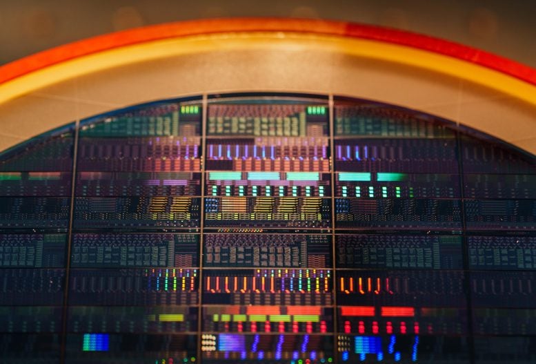
“Sandia has one of the most flexible foundries in the world, not only in microelectronics but also in photonics,” Lukens said, referring to the MESA complex. “Sandia can fabricate small photonic integrated circuits that can realize the same capabilities as a big square meter-size optical table.”
Sandia’s National Security Photonics Center offers a wide variety of component and platform technologies, with a portfolio of more than 50 issued patents in integrated photonics.
Advancements in Quantum Photonics
Spatial beam splitters, which take photons and split them in two directions, are fundamental components in quantum photonics.
“In this frequency encoding paradigm, we need to create special types of beam splitters that instead take one color of light and split it into two colors,” Otterstrom said. “What we’ve developed here at Sandia, in collaboration with professor Peter Rakich’s team at Yale University, are these very efficient novel phase modulator devices.”
The devices are based on suspended silicon waveguides that convey light and gigahertz soundwaves, which are generated by co-integrated aluminum nitride electro-mechanical transducers.
“The result is highly flexible optomechanical structures that acousto-optically split a photon into multiple frequencies. This allows you to do quantum information processing on a much higher dimensional space,” Otterstrom said. “You can think about it as the light’s color can actually carry the quantum information.”
Future Prospects and Applications
Lukens said his goal is to move work from proof-of-principle experiments to deployment in quantum networks.
“In order to do that, we need systems with lower loss than what we can achieve today with commercial devices, and we need systems that are a bit cheaper,” Lukens said. “If we can realize those capabilities on chip, now we’re talking about a much more practical and plausible way to do quantum networking.”
Otterstrom has been guiding Lukens to acquire components, such as microscopes and optical mounts, to use the Sandia-built photonic integrated circuits in a testbed at the university’s lab.
A Milestone in Quantum Collaboration
The collaboration is paying off. Sandia’s Laboratory Directed Research program has awarded $17 million to advance the team’s work in frequency-based quantum photonics. The funding comes in the form of a Grand Challenge program called Error-Corrected Photonic Integrated Qubits, or EPIQ.
“Without the partnership between Sandia and Arizona State University, we would probably not have the EPIQ Grand Challenge in its current shape and form,” said Paul Davids, the principal investigator on the project. “Nils’ outreach to Joe Lukens began our first foray into the ideas around frequency-encoded photonic qubits. His thoughtful leadership in this area and Joe Lukens’ prior work and expertise are central to the EPIQ Grand Challenge.”
Otterstrom said the funding will enable large-scale implementation and integration of the device physics explored in the early collaboration with Arizona State University to create a useful photonic qubit that can be error-corrected.
Supporting Quantum Tech Development
In addition to participating in the Quantum Collaborative, Sandia offers the MESA complex’s microelectronics prototyping capabilities as a core partner of the Southwest Advanced Prototyping Hub. SWAP Hub, which is also led by Arizona State University, is one of eight Microelectronics Commons Hubs across the country. The Microelectronics Commons is funded by the CHIPS and Science Act enacted by Congress to jumpstart American competitiveness in the semiconductor industry and reduce dependence on foreign suppliers.