
Researchers at Oak Ridge National Laboratory and Korea’s Sungkyunkwan University are using advanced microscopy to nanoengineer promising materials for computing and electronics in a beyond-Moore era.
Historically, computers have become faster and more powerful by Moore’s Law, an observation that technology advances as transistor sizes shrink. Today’s nanometer-scale transistors are reaching practical limits and new approaches are needed to scale existing technology.
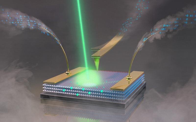
A team at ORNL’s Center for Nanophase Materials Sciences has applied a focused beam of helium ions to locally tailor ferroelectricity in a metal oxide thin film, enhancing a useful property for transistors and memory. Results published in Science show how light ion microscopy can unlock unique functionalities in materials and create new pathways to design future devices.
“This project highlights the advanced ion beam and scanning probe capabilities available to CNMS users, which open new frontiers to locally control and understand materials properties on the nanoscale,” said ORNL’s Liam Collins.
Self-driving microscopes discover shortcuts to new materials
Seunghun Kang et al, Highly enhanced ferroelectricity in HfO 2 -based ferroelectric thin film by light ion bombardment, Science (2022). DOI: 10.1126/science.abk3195
Oak Ridge National Laboratory
Citation:
Using advanced microscopy to nanoengineer new materials for computing and electronics (2022, June 2)
retrieved 2 June 2022
from https://phys.org/news/2022-06-advanced-microscopy-nanoengineer-materials-electronics.html
This document is subject to copyright. Apart from any fair dealing for the purpose of private study or research, no
part may be reproduced without the written permission. The content is provided for information purposes only.